
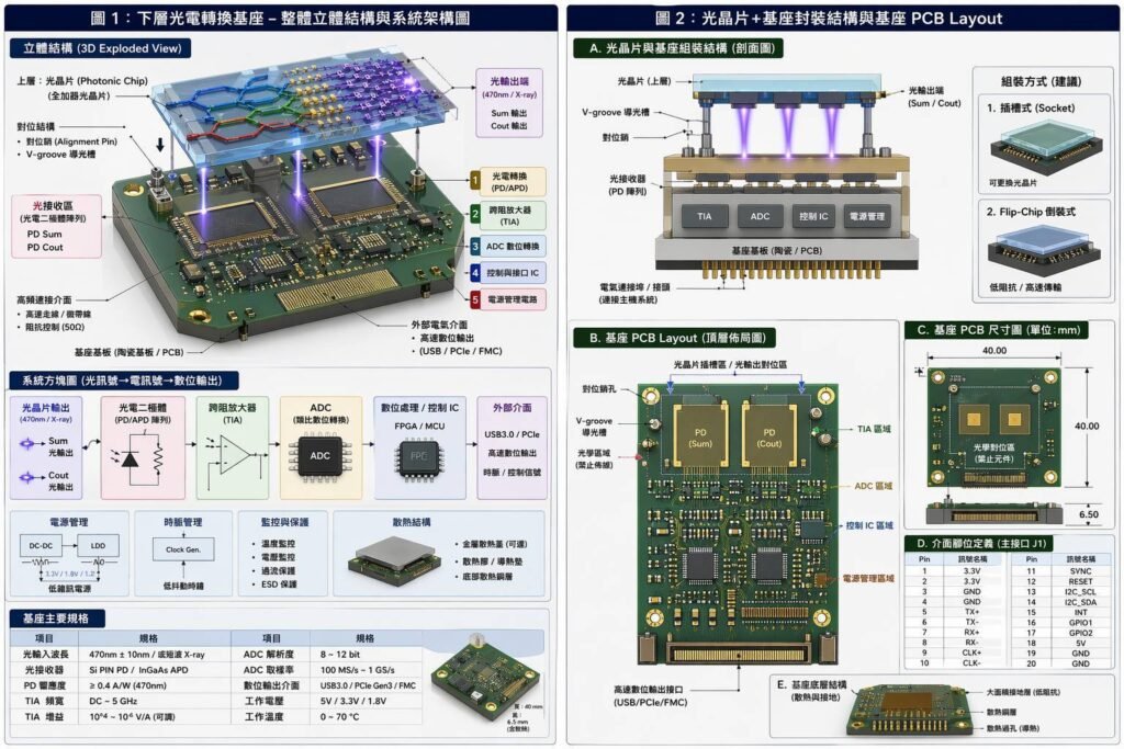
Figure 1. 3D schematic diagram of a photonic chip, with the upper layer being the photonic chip and the lower layer being the photoelectric conversion base.
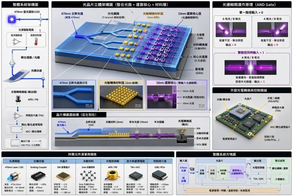
Figure 2. 3D architecture diagram of photonic chip
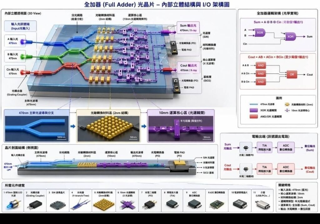
Figure 3. Full adder optical chip – Internal 3D structure and I/O architecture diagram
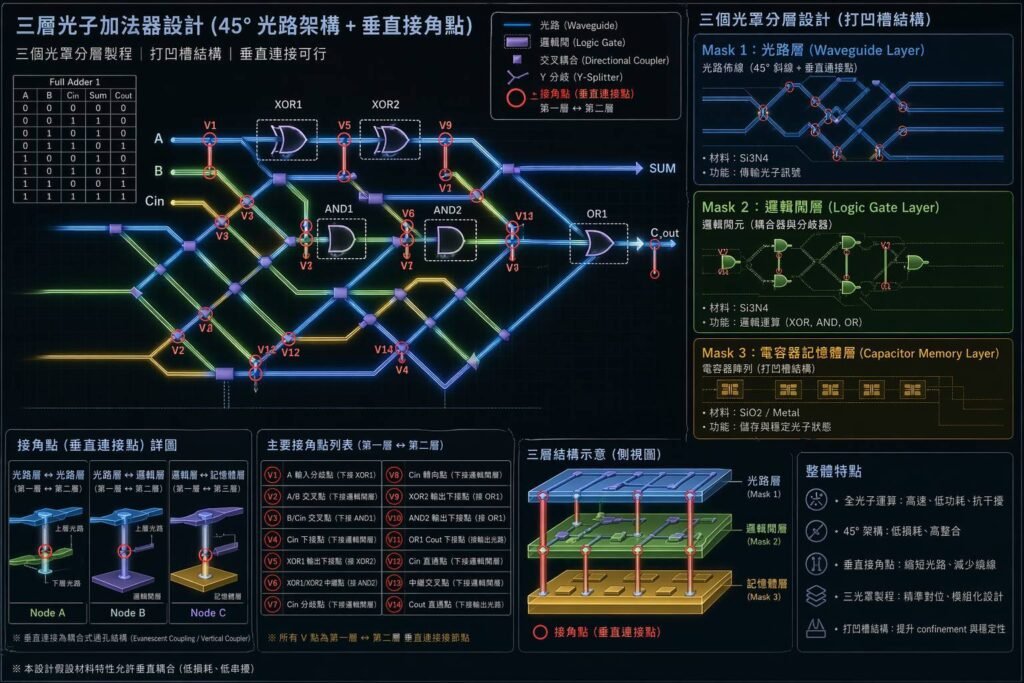
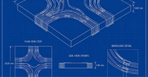
Figure 4. Example diagram of a full adder photonic wafer structure
Example of a Full Adder Photonic Chip Structure:
This design is based on a full adder, completely transforming traditional electronic circuitry into a 45-degree optical path architecture. To demonstrate the three-dimensional integration capabilities of photonic chips, the original planar structure is further optimized into a three-layer stacked design:
Top Layer : Optical Path Layer
Middle Layer : Logic Gate Layer
Bottom Layer : Memory Layer
The entire fabrication process utilizes three different photomasks.
Compared to electronic chips that often require dozens of layers, photonic chips can achieve high-efficiency computation with only three layers. Combined with photonic memory, its computational performance can be increased by hundreds of thousands of times. Because light completes access at near-instantaneous speeds, its actual speed is difficult to measure accurately using traditional methods.