
Computing Architecture and Fabrication Technologies of 2 nm Optical Quantum Chips
From Electronic Bottlenecks to a Light-Speed Future:
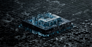
Photonic quantum chips (Fig. 1) use photons instead of electrons as carriers of information. Photons have nearly zero mass, propagate at much higher speeds, and significantly reduce energy loss and heat generation. By forming optical pathways using photosensitive materials and controlling signal transmission through laser sources, photonic quantum chips enable high-speed, low-power data processing. Their fabrication process is relatively simpler and offers more stable manufacturing yields. Moreover, photonic quantum chips perform logic operations based on the presence or absence of light, rather than electrical current.

Figure 1. Core technologies of photonic quantum chips vs. electronic chips
Dr. Fang’s photonic quantum chip is built around two key modules: photosensitive and photoresist. It can be fabricated on standard silicon wafers, and alternatively on substrates such as ceramics or optical glass (Patent No.: TWI693498, Claim 5) [2]. The design logic is described as follows:
Optical Path Key Technology – Replacing Copper Interconnects with “X Photon Material”
Optical Channel Module:
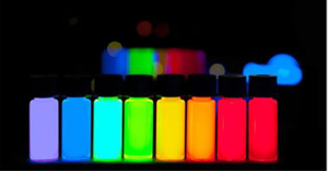
Dr. Fang’s proprietary X Photon material is used as the chip’s internal optical channel module. This enables ultra-fine optical structures down to 2 nm, reducing photon channel wavelengths to an average of 2 nm (Fig. 2) [1]. The design allows photons to transmit with nearly zero loss, no physical resistance, and therefore no heat generation. (more..)
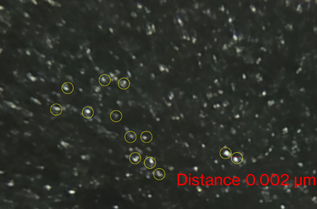
Fig 2. The white light spot represents the 2-nm photon wavelength.
Light Source Module
Dr. Fang’s design for the light source module uses LEDs (or lasers) as the emission source. Following the binary design principle of the photonic quantum chip, two sets of LED emitters are positioned at the front of the optical channel module to work in conjunction with the optical logic gates (Patent No.: TWI693498, Claim 6) [2].
Core of Computation: Photoresist Material – Simulating Logic “0” and “1” via Light Transmission
Once the optical channel transmits photonic signals, the next step is computation. Dr. Fang’s photoresist material is used to construct optical logic gates. The operation principle is as follows:
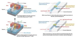
Operation Mechanism of Optical Logic Gates:
Two sets of LED emitters (here illustrated as laser sources) are positioned at the front of the optical channel module. When photon signals reach the photoresist units, the system determines whether the photons can pass through or not, simulating the 0 and 1 logic of electronic chips (Patent No.: TWI693498, Claim 5) [2].
Logic “0”:
If only the first laser source is active while the second is off, the photon signal reaches the photoresist unit. Because only one beam is present, it cannot pass through the photoresist, so no light is detected at the back end (no transmission). The system interprets this as logic 0 (Fig 3).
Logic “1”:
When both the first and second laser sources emit a laser beam and enter the optical path, the photon signals reach the photoresist unit. Since both laser beams arrive simultaneously, they penetrate the photoresist, allowing the light signal to pass through and be detected at the back end (light transmission). The system interprets this as logic 1 (Fig. 4). (more..)
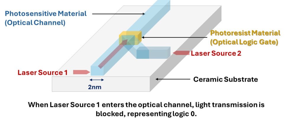
Fig. 3. Operation Mechanism of Optical Logic Gates – Illustration of Logic “0
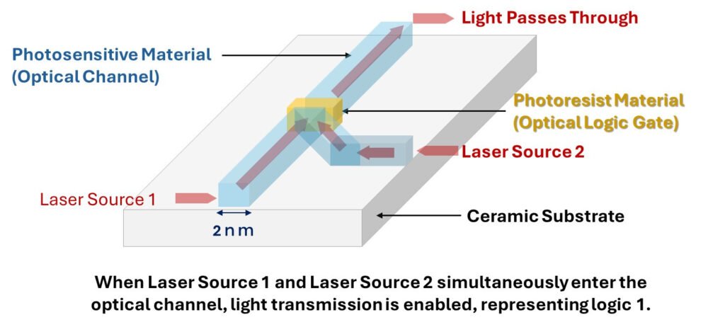
Fig. 4. Operation Mechanism of Optical Logic Gates – Illustration of Logic “1”
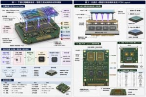
Key Steps for Integrating Photonic Quantum Chips with Semiconductor Processes
Next, we will explain how Dr. Fang’s developed photosensitive and photoresist materials can be applied in current semiconductor manufacturing. The integration process of photonic quantum chips with standard semiconductor fabrication is as follows (Figure 5):
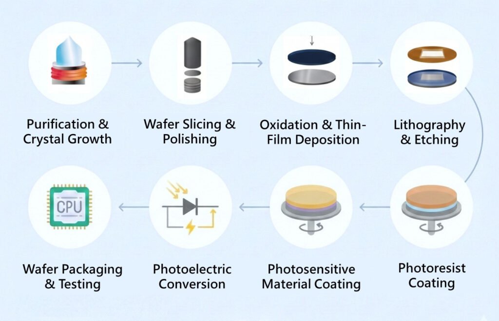
Fig. 5. Integration Process of Photonic Quantum Chips with Semiconductor Fabrication