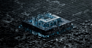

Photonic Quantum Chips Core Design
Computing Architecture and Fabrication Technologies of 2 nm Optical Quantum Chips
Outline
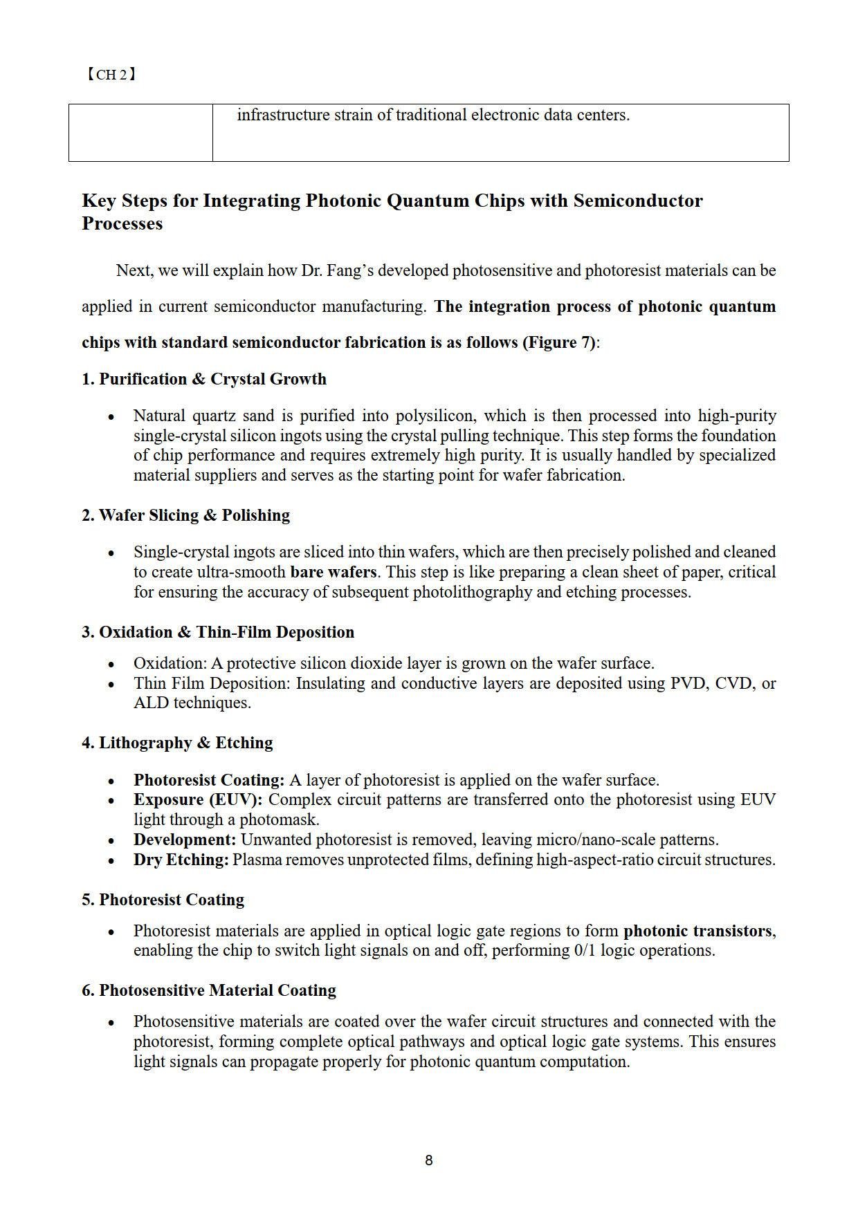
From a manufacturing perspective, the process directly replaces traditional metal interconnects (copper wiring) with photosensitive materials within conventional chip fabrication flows. Unlike silicon transistors, which suffer from severe leakage current and physical scaling limits at advanced nanometer nodes, optical quantum chips rely on chemically stable photoresist materials for control. This “optical wall” design, governed by chemical material properties, is immune to electromagnetic interference and completely avoids the leakage and thermal loss issues that plague electronic transistors at the 2-nanometer node. As a result, production yield is significantly improved, while computing performance reaches up to 1,000 times that of comparable electronic chips.
In terms of computing logic, photoresist materials function as optical logic gates. Binary states (1 and 0) are precisely represented by whether laser light is allowed to pass or is blocked. When two laser beams enter the structure simultaneously, the photoresist unit becomes transparent, corresponding to logic “1.” When only a single laser beam is present, light cannot pass, corresponding to logic “0.” The patent portfolio for this technology covers 26 countries and regions, including Taiwan, China, the United States, Japan, South Korea, India, Hong Kong, Spain, and 18 European Union member states under the UPC system .
Photonic Quantum Chip Design
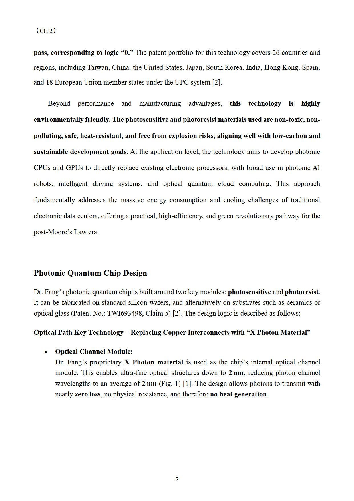
Optical Channel Module:
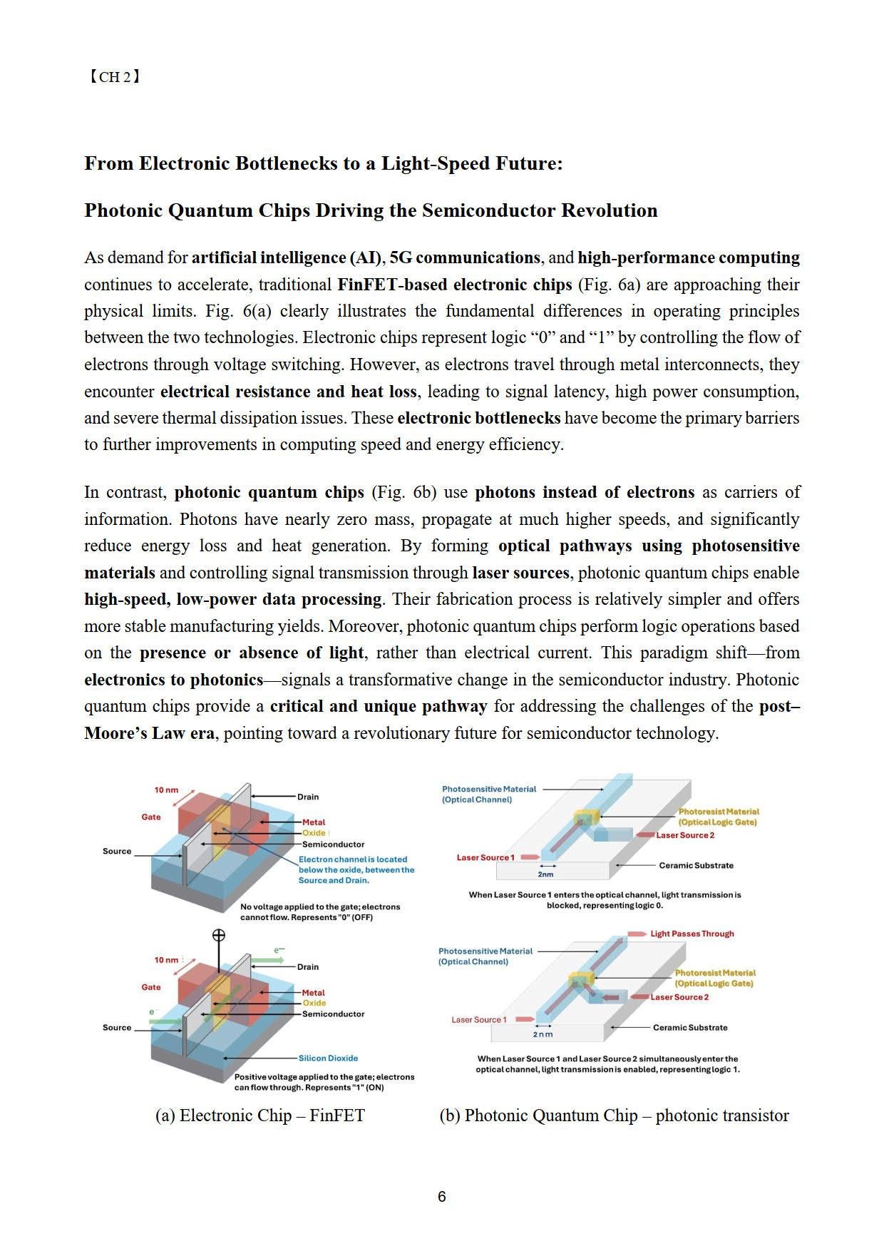
Dr. Fang’s proprietary X Photon material is used as the chip’s internal optical channel module. This enables ultra-fine optical structures down to 2 nm, reducing photon channel wavelengths to an average of 2 nm (Fig. 1) [1]. The design allows photons to transmit with nearly zero loss, no physical resistance, and therefore no heat generation.
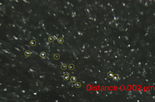
Fig. 1. White light spots (indicated by circles) correspond to photons with a 2 nm wavelength.
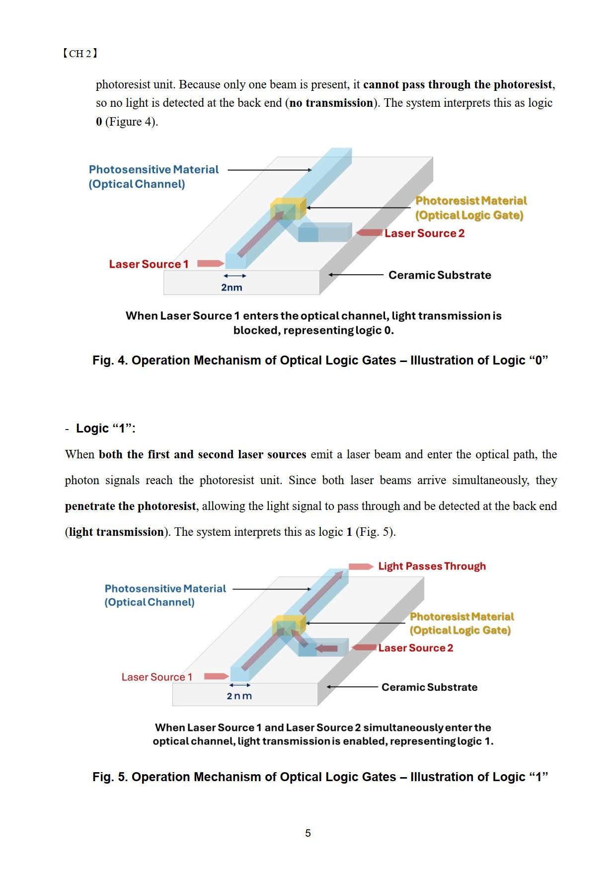
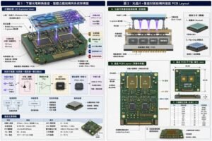
Light Source Module
Dr. Fang’s design for the light source module uses LEDs or lasers source as the emission source. Following the binary design principle of the photonic quantum chip, two sets of lasers diode emitters are positioned at the front of the optical channel module to work in conjunction with the optical logic gates (Patent No.: TWI693498, Claim 6)
Logic “0”:
If only the first laser source is active while the second is off, the photon signal reaches the photoresist unit. Because only one beam is present, it cannot pass through the photoresist, so no light is detected at the back end (no transmission). The system interprets this as logic 0 (Figure 2).
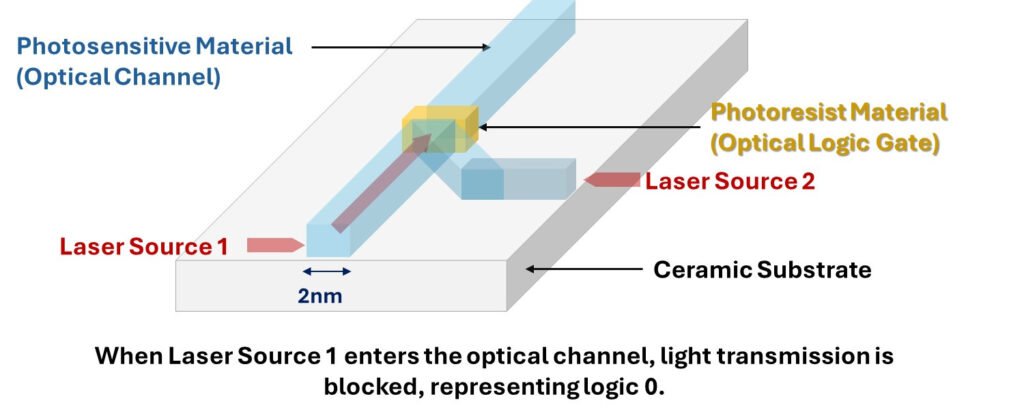
Fig. 2. Operation Mechanism of Optical Logic Gates – Illustration of Logic “0”
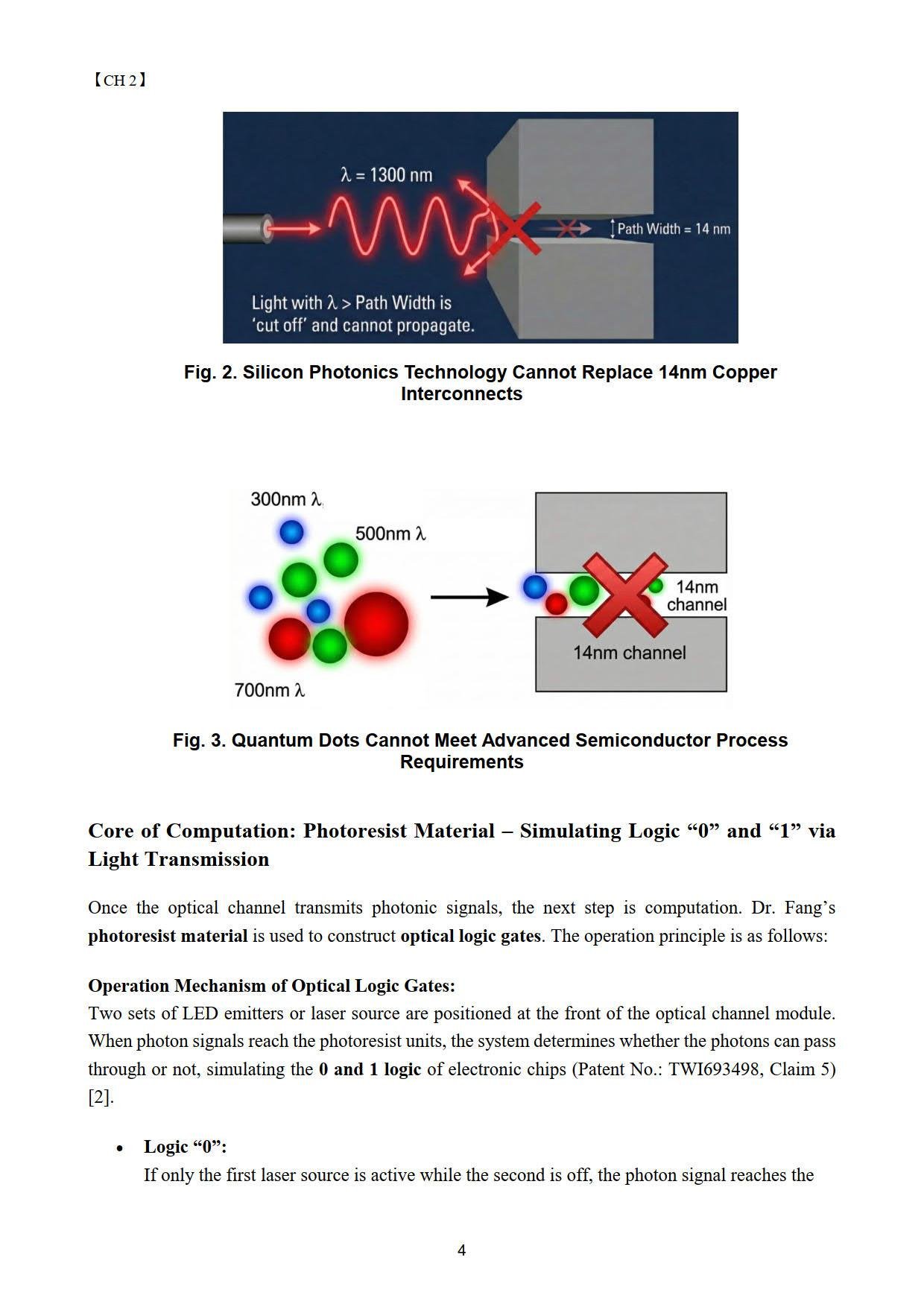
Logic “1”:
When both the first and second laser sources emit a laser beam and enter the optical path, the photon signals reach the photoresist unit. Since both laser beams arrive simultaneously, they penetrate the photoresist, allowing the light signal to pass through and be detected at the back end (light transmission). The system interprets this as logic 1 (Fig. 3).
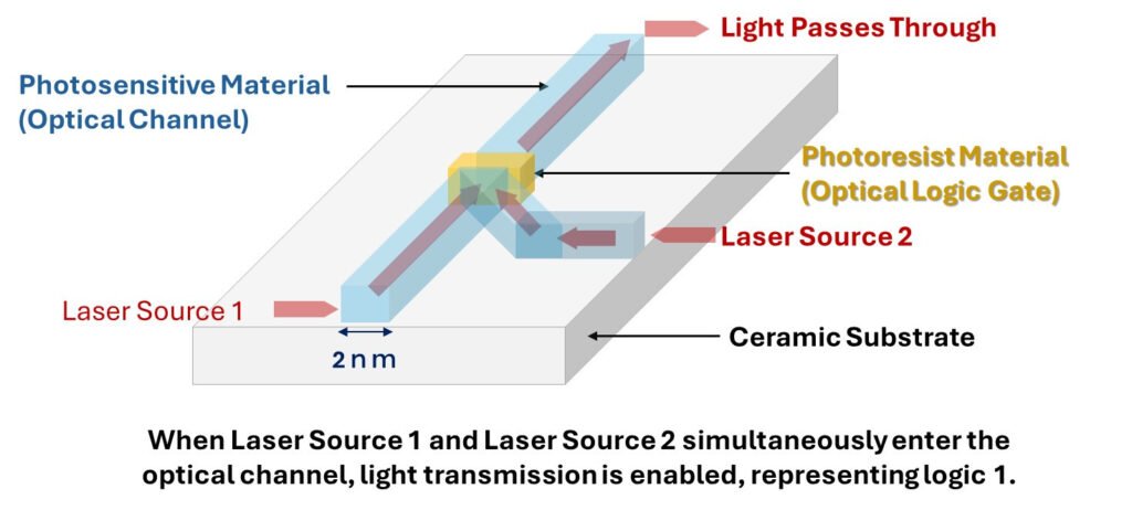
Fig. 3. Operation Mechanism of Optical Logic Gates – Illustration of Logic “1”
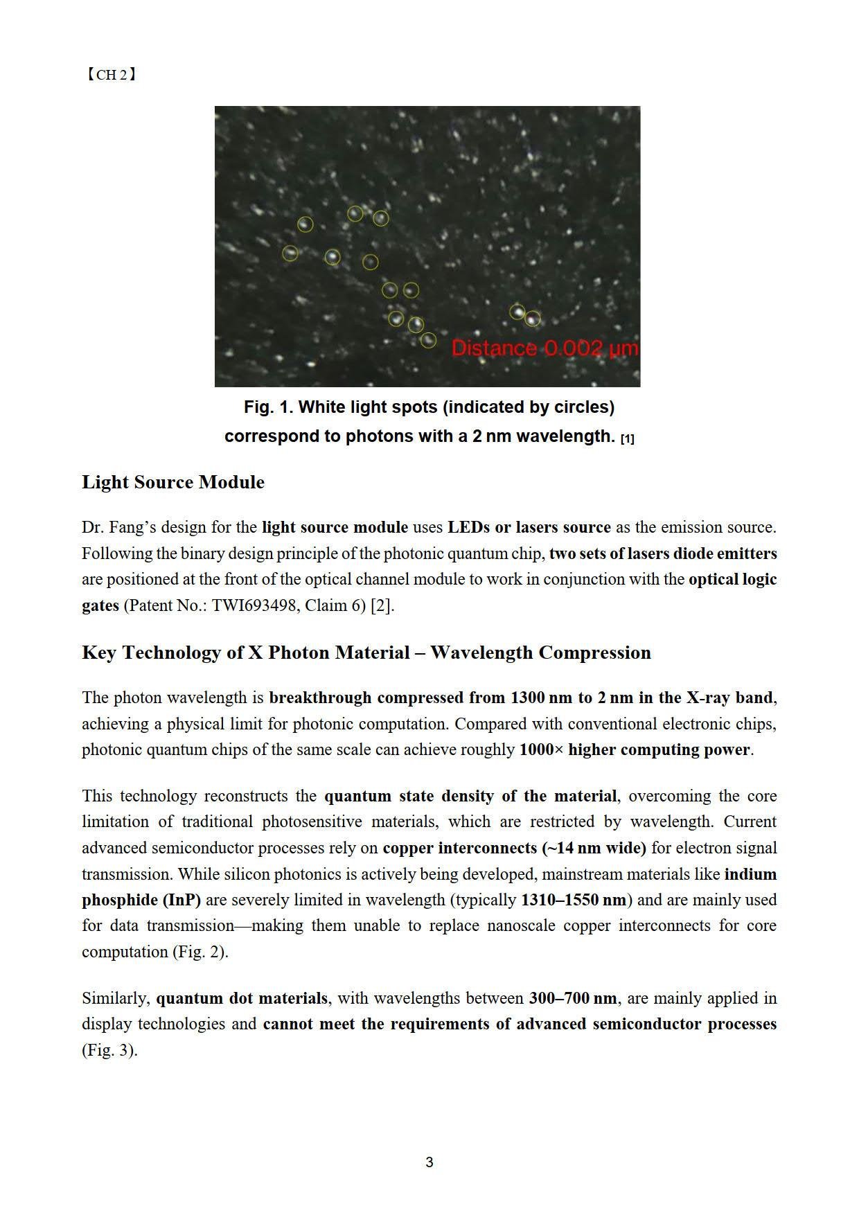
From Electronic Bottlenecks to a Light-Speed Future:
In contrast, photonic quantum chips (Fig. 4a) use photons instead of electrons as carriers of information. Photons have nearly zero mass, propagate at much higher speeds, and significantly reduce energy loss and heat generation. By forming optical pathways using photosensitive materials and controlling signal transmission through laser sources, photonic quantum chips enable high-speed, low-power data processing. Their fabrication process is relatively simpler and offers more stable manufacturing yields.
This paradigm shift—from electronics to photonics—signals a transformative change in the semiconductor industry. Photonic quantum chips provide a critical and unique pathway for addressing the challenges of the post–Moore’s Law era, pointing toward a revolutionary future for semiconductor technology.
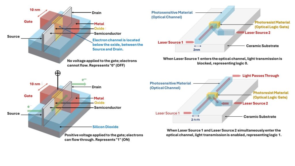
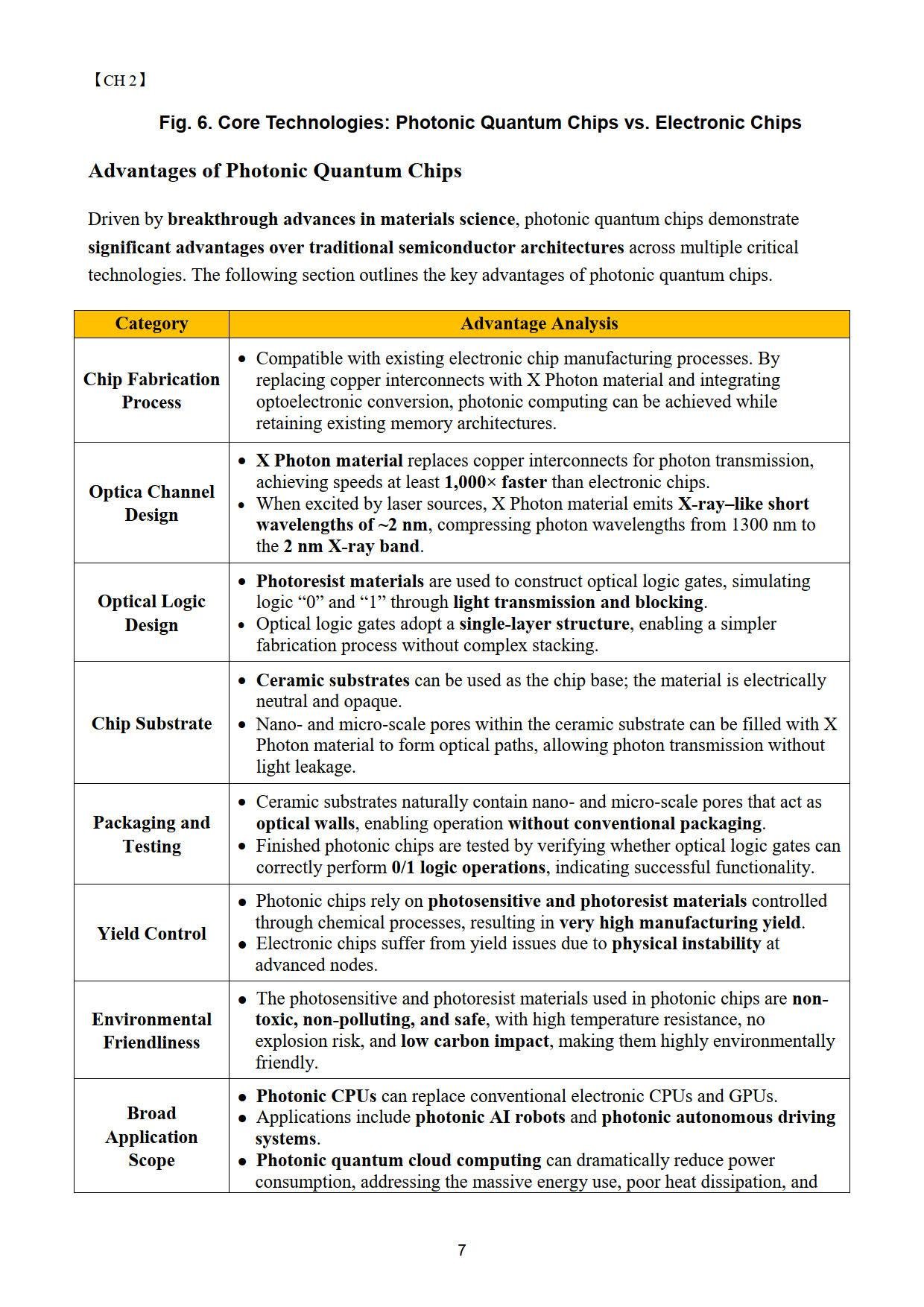
Fig. 4. Core Technologies: Photonic Quantum Chips vs. Electronic Chips
Advantages of Photonic Quantum Chips
| Category | Advantage Analysis |
| Chip Fabrication Process | Compatible with existing electronic chip manufacturing processes. By replacing copper interconnects with X Photon material and integrating optoelectronic conversion, photonic computing can be achieved while retaining existing memory architectures. |
| Optica Channel Design | X Photon material replaces copper interconnects for photon transmission, achieving speeds at least 1,000× faster than electronic chips.When excited by laser sources, X Photon material emits X-ray–like short wavelengths of ~2 nm, compressing photon wavelengths from 1300 nm to the 2 nm X-ray band. |
| Optical Logic Design | Photoresist materials are used to construct optical logic gates, simulating logic “0” and “1” through light transmission and blocking.Optical logic gates adopt a single-layer structure, enabling a simpler fabrication process without complex stacking. |
| Chip Substrate | Ceramic substrates can be used as the chip base; the material is electrically neutral and opaque.Nano- and micro-scale pores within the ceramic substrate can be filled with X Photon material to form optical paths, allowing photon transmission without light leakage. |
| Packaging and Testing | Ceramic substrates naturally contain nano- and micro-scale pores that act as optical walls, enabling operation without conventional packaging.Finished photonic chips are tested by verifying whether optical logic gates can correctly perform 0/1 logic operations, indicating successful functionality. |
| Yield Control | Photonic chips rely on photosensitive and photoresist materials controlled through chemical processes, resulting in very high manufacturing yield.Electronic chips suffer from yield issues due to physical instability at advanced nodes. |
| Environmental Friendliness | The photosensitive and photoresist materials used in photonic chips are non-toxic, non-polluting, and safe, with high temperature resistance, no explosion risk, and low carbon impact, making them highly environmentally friendly. |
| Broad Application Scope | Photonic CPUs can replace conventional electronic CPUs and GPUs.Applications include photonic AI robots and photonic autonomous driving systems.Photonic quantum cloud computing can dramatically reduce power consumption, addressing the massive energy use, poor heat dissipation, and infrastructure strain of traditional electronic data centers. |
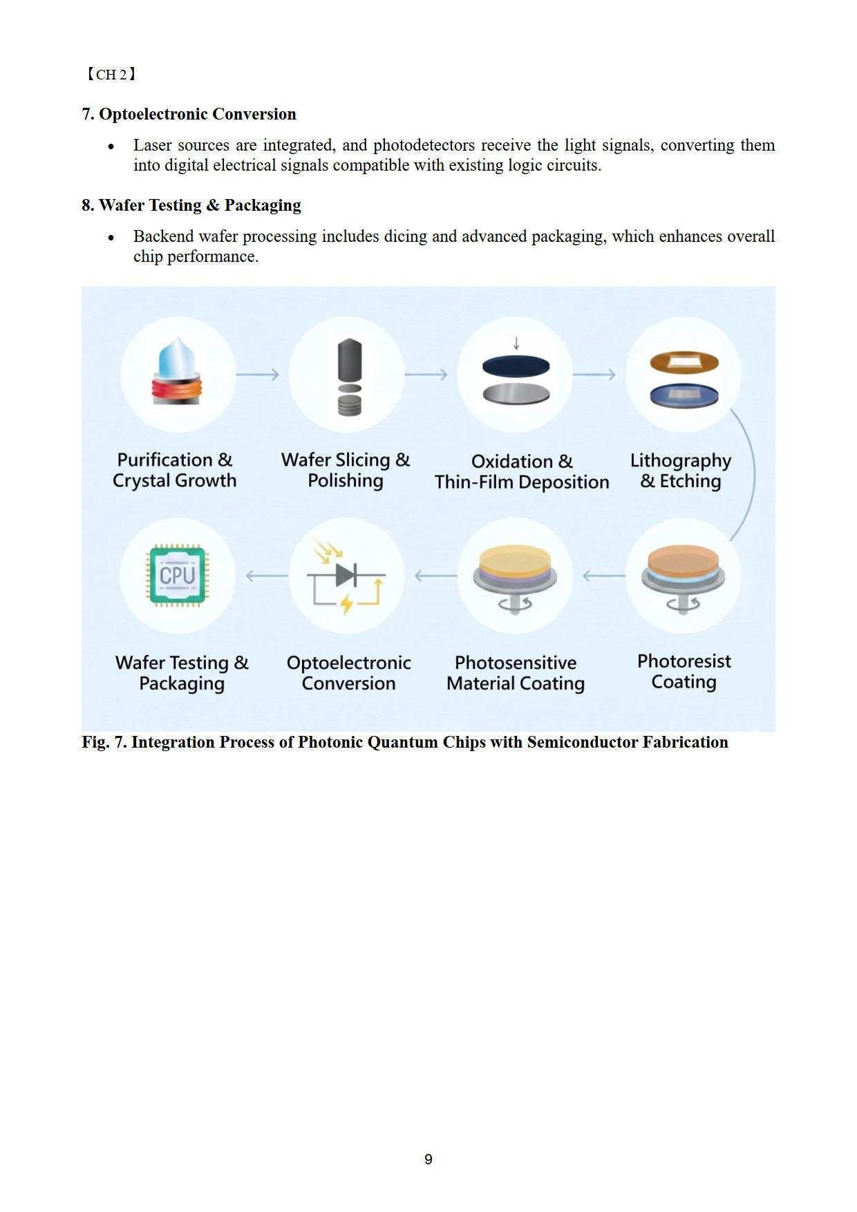
Key Steps for Integrating Photonic Quantum Chips with Semiconductor Processes
Next, we will explain how Dr. Fang’s developed photosensitive and photoresist materials can be applied in current semiconductor manufacturing. The integration process of photonic quantum chips with standard semiconductor fabrication is as follows (Figure 5):
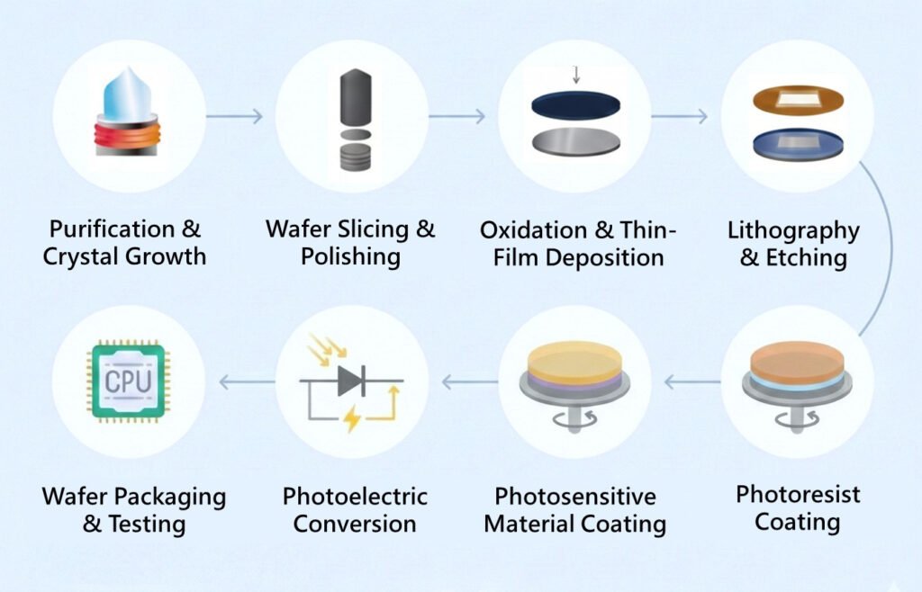
Fig. 5. Integration Process of Photonic Quantum Chips with Semiconductor Fabrication
Photonic Chip vs Electronic Core Design