
Quantum Computing & AI
Photonic Quantum Processing
Harnessing the speed of light for next-generation computing
Our Photonic Quantum Chip technology merges advanced silicon photonics with quantum mechanics to redefine computational limits. By utilizing particles of light (photons) rather than traditional electrons, we eliminate thermal bottlenecks and enable lightning-fast, energy-efficient data processing.
Developed through precision nanoscale fabrication, our photonic architecture is engineered to achieve:
- Room-temperature quantum coherence
- Ultra-low latency and minimal signal loss
- Massively scalable qubit entanglement
- Seamless integration with existing optical networks
Our long-term vision is to embed this advanced photonic infrastructure directly into intelligent systems, powering exponentially faster, more efficient, and highly scalable AI ecosystems.
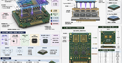
Photonic Quantum Chip
Chips
Availability & Collaboration
We are open to:
- Retail partnerships
- Luxury brand collaborations
- Custom design projects
- Material licensing discussions
Photonic Quantum Chip Announcement
Longserving Technology Announcement: World's First Photonic Chip Demonstration Factory Launched
Longserving Technology officially announces a major breakthrough in photonic chip manufacturing technology.
We have successfully established independent equipment and core process capabilities, moving beyond the traditional semiconductor manufacturing ecosystem. By eliminating the need for legacy systems—including photolithography machines (EUV/DUV), etching equipment, and photoresist materials—we have pioneered a next-generation photonic chip production model, bringing fundamental transformation to the computing industry.
Based on this foundation, Longserving Technology possesses the following key capabilities:
- Independent R&D and Manufacturing of Photonic CPUs
- Independent R&D and Manufacturing of Photonic Memory
- Integration of Photonic Computing and Photonic Memory Storage: Achieving processing power potentially 10,000 times greater than existing electronic CPUs.
Simultaneously, we are fully committed to establishing a Photonic Chip Demonstration Factory in Taiwan, creating a world-leading industrial hub for photonic technology.
Invitation for Collaboration
LongServing Technology welcomes partners dedicated to the development of Photonic IC design and photoelectric conversion components to collaborate with us:
- Photonic IC Design
- Photoelectric Conversion Technology
- Related Specialized Components
We look forward to joining forces with industry leaders to co-create a new era of photonic computing.
Current Areas of Development
(The following responses are provided by Dr. Ko-Cheng Fang, CEO of LongServing Technology)
Q1. Can this patented solution be understood as a photonic processor based on binary logic (i.e., a photonic digital chip)?
A1: Yes. This is a binary photonic computing chip.
Q2. How are ecosystem and compatibility addressed? Since this approach replaces electronic computation with photonic computation, would CPUs/GPUs, instruction sets, and compilers need to be redesigned? Are there scenarios where it cannot directly replace existing processors? If so, how would adoption be promoted?
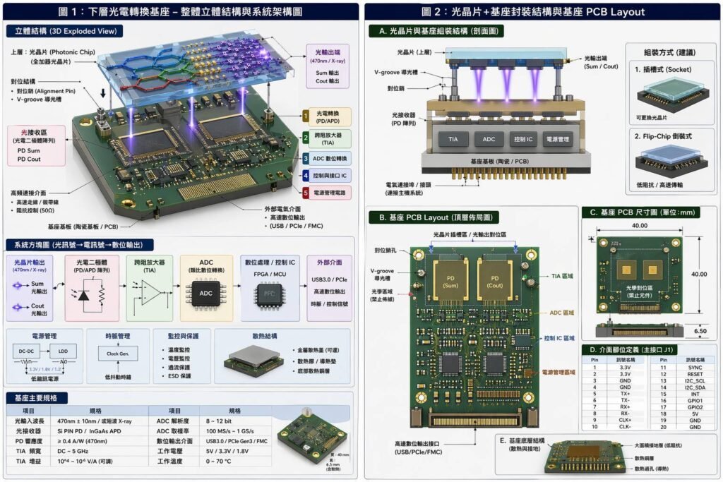
A2: Photoelectric conversion has already been demonstrated in TSMC’s silicon photonics technology—for example, replacing electronic data transfer between chips and memory with photonic transmission.
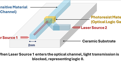
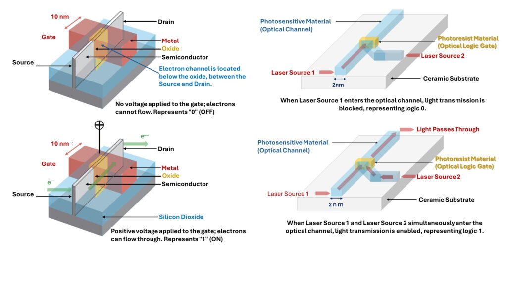
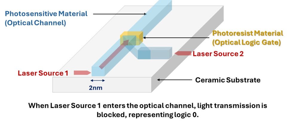
However, our design goes further by applying photonics directly within the computational core. We replace traditional copper interconnects with X-photonic materials (invented by Dr. Ko-Cheng Fang, CEO of LongServing Technology), and utilize photoresist materials as logic gates.
The overall architecture follows conventional electronic design principles; the only change is replacing electrons with photons as the carrier. At the I/O level, photoelectric conversion (optical-to-electrical and electrical-to-optical) is used, ensuring that existing software instructions and electronic systems remain fully compatible without modification.
Q3. How is loss from photoelectric conversion addressed? Page 7 of “Beyond Moore’s Law: Computational Architecture and Fabrication Technology of 2nm Photonic Quantum Chips” mentions a “photoelectric conversion module.” Does this imply multiple electrical–optical–electrical conversions and associated latency or loss?
A3: The relatively slow speed of electron transmission in copper interconnects is due to a “domino effect,” where one electron pushes another. This makes electron-based transmission inherently slower—by approximately a factor of 1,000—compared to photons.
Additionally, electronic computation is susceptible to electromagnetic interference, which further limits performance. At the nanoscale, quantum tunneling effects also emerge, causing ambiguity in binary signals (0 and 1), often requiring software-level correction.
Photons do not suffer from these limitations. Photoelectric conversion itself is straightforward and occurs only at input/output stages. The computation process is entirely photonic, with no electrons involved, resulting in significantly improved speed and energy efficiency.
The so-called “photoelectric conversion module” is a patent term. In practice, it is simply a coating layer within a logic gate. For electrical-to-optical conversion, existing LEDs can be used. These are based on well-established III-V semiconductor materials with phosphorus doping, which are already widely applied.
For optical-to-electrical conversion, the principle is similar to solar panels, where photons striking a material generate electrical current. These are mature and widely adopted technologies.
Q4. The project describes photonic CPUs and GPUs that directly replace electronic processors. Does this imply building a complete computing architecture (control units, processing units, etc.), rather than just accelerating specific algorithms? Will software differ from existing systems, or is software migration supported?
A4: On the software side, no changes are required. All instruction sets remain the same—we only modify the hardware.
Imagine removing the CPU from a smartphone and replacing it with a photonic CPU. With identical pin configuration, it can be installed and function immediately—while delivering approximately 1,000 times faster performance. That captures the essence of our approach.
Q5. What is the current level of technological maturity? The project mentions “2nm X-ray wavelengths” and “photonic logic gates”—have these reached scalable commercial validation? What are the validation scenarios and scale?
A5: In terms of photonic materials, we have already conducted laboratory imaging and observed X-ray short wavelengths averaging around 2nm. Photonic logic gate signals (0 and 1) have also been successfully tested, although they cannot be captured by electron microscopy.
In mask fabrication, our company has successfully produced 7nm and 10nm photonic pathways, indicating that our capabilities surpass global leading mask technologies, including those of TSMC. Current mask technologies are typically in the 90nm to 68nm range, and even the most advanced semiconductor processes cannot achieve 7nm and 10nm photonic pathways in this manner.
Due to regulatory constraints, our photonic chip manufacturing must remain above 14nm. However, this is not a limitation, as current electronic chip copper interconnects are also around the 14nm node.
As for mass production, it has not yet commenced. We are currently seeking foundry partners. With only partial modifications to their existing processes, mass production can be achieved.
Q6. What is your commercialization and deployment strategy? What are the key entry points, and how do you envision different growth phases (introduction, expansion, maturity) in terms of demand, capacity, and pricing?
A6: We are currently integrating foundry partners across the supply chain. In Taiwan, this process is already underway and progressing smoothly. In Mainland China, integration is also in progress, as localization is required for that market.
We plan to first produce photonic chip samples for testing. If successful, performance is expected to be 1,000 to 10,000 times faster than electronic chips, at which point we will enter the order-taking phase.
Since production capacity and equipment are already in place, once technical validation is complete, a strong order-shifting effect is expected. At that stage, traditional electronic chip supply chains that fail to transition in time will face inevitable market displacement.
Q7. For Mainland China foundries, will your company establish production facilities locally? If not, how will you ensure smooth collaboration?
A7: The location of production facilities should be determined by the manufacturing ecosystem and foundry partners themselves. LongServing Technology will focus on system integration and core capabilities in Taiwan. For the Mainland China market, we maintain an open and collaborative approach. The global semiconductor landscape is increasingly shaped by geopolitical competition, particularly between the U.S. and China, extending into AI and broader technology domains. Failure to act early may result in falling behind or being phased out entirely.
Optical Quantum Chip
6 min read
Introduction to Optical Quantum Chips
From Electronic Bottlenecks to a Light-Speed Future:
Optical Quantum Chip
4 min read
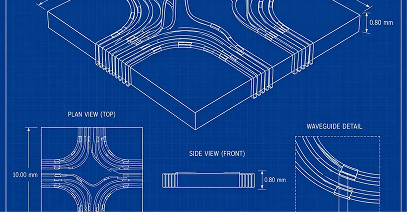
Schematic diagram of photonic chip structure
This design is based on a full adder, completely transforming traditional electronic circuitry into a 45-degree
Optical Quantum Chip
4 min read
Refuting AI Misconceptions about Photonic Chips
Advanced material engineering meets sustainable luxury in our newest manufacturing breakthrough.
Optical Quantum Chip
6 min read
Optical Quantum Chip Core Design
Our latest experiments demonstrate coherence times that exceed previous benchmarks significantly.

Optical Quantum Chip
4 min read
Optical Quantum Chip Material Technology
Advanced material engineering meets sustainable luxury in our newest manufacturing breakthrough.
Introduction to Optical Quantum Chips
Computing Architecture and Fabrication Technologies of 2 nm Optical Quantum

Refuting AI Misconceptions about Photonic Chips
Can LongServing Technology’s Photonic CPU Truly Outperform Electronic CPUs? When
Optical Quantum Chip Core Design
Photonic Quantum Chips Core Design Computing Architecture and Fabrication Technologies
Schematic diagram of photonic chip structure
Figure 1. 3D schematic diagram of a photonic chip, with